I’m documenting this primarily for my own purposes, should I need to do this again at some point. I’m also doing it to share the information, since it might help a suitably qualified individual repair one of these inverters. This repair and testing isn’t to be attempted unless you fully understand all of the risks. You could end up being electrocuted if you don’t take the necessary precautions. An RCD won’t save you if you mess this up.
Let’s get into it!
“No AC Connection” it says, innocently enough.
It’s lying and withholding information about the horror that has unfolded inside.
There’s a 20A, 3AG HRC ceramic fuse, near to where the mains enters the power board. It’s blown.
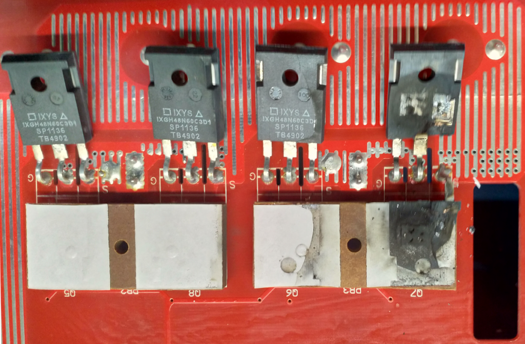
One instinctively looks around to find the actual inverter circuitry (the H-bridge), quietly hoping it’s not an expensive pre-made inverter module. Thankfully, it wasn’t. Just a heap of mostly discreet components combined with four IGBT’s to form a H-bridge. So, it’s serviceable at the component level, which is nice.
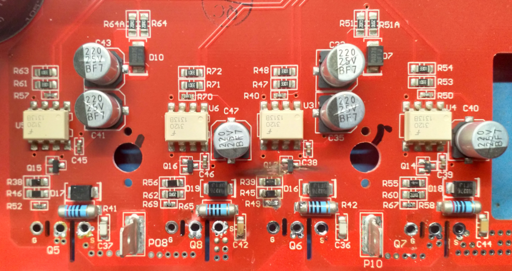
There’s a skid mark across part of the PCB down there, where one of the small transistors has pooped itself. There’s another one with the top blown clean off. There’s multiple burnt and otherwise damaged SMD resistors and a couple of damaged but still functional ceramic capacitors. At this stage, I pretty much know what’s happened. At least one of those IGBT’s has failed short and/or exploded and the gate pin has lost it’s insulation property (that’s the I in IGBT). That’s a problem, because the IGBT’s gates are generally fairly low voltage – 15-30V, but the IGBT itself can often be switching voltages in the hundreds of volts. In an inverter like this, it could be switching 500V, since that’s the maximum voltage the inverter is rated for – but you’d be ill advised to run it anywhere near that.
There’s four FOD3120 devices down there as well. They’re gate drive optocouplers for the four IGBT’s, but there’s a problem. The isolation barrier has been compromised and some of the low voltage circuitry has been damaged.
There’s a rectangular cut-out in the PCB where a couple of wires go to a thermistor attached to the heatsink under the power board. There’s quite a decent black mark down there as well.
H-Bridge Circuitry (damaged):
Second hand units on Gumtree? Not at the moment.
Schematics available? Couldn’t find any.
Continuing the diagnosis then. The path the current took via R51/R51A leads back to a low voltage power supply. Everything there looks physically intact and everything checks out OK with a multimeter, so that’s good news. The logic board still works when there’s power from the solar panels connected, so I’m thinking it might have a chance of being repairable.
Since the low voltage power supply also supplies power to all of the FOD3120 optocouplers and is also used for driving the LEDs in those optocouplers, they’re possibly all damaged. Tracing back where the LED side of the optocouplers are driven from leads me to the logic board, as expected. There’s a ULN2003A there, near the IDC header. Poking around the ULN2003A didn’t reveal any obvious damage, but I started the repair by replacing that chip, not taking any chances. I had them in stock, since they’re about as common as dirt.
I then went about identifying all of the components in the H-bridge circuitry. Since it’s a H-bridge, the “high” side and “low” sides are duplicated. Thankfully, one high and one low section of circuitry survived, and due to this, I decided to commit to doing the repair, since all of the damaged components were going to be identifiable.
Components were ordered and the repair was done. I replaced every component in the H-bridge circuitry and some others as well, mostly being cautious. I’m $120 in and I’ve spent the best part of a day on it. I don’t want to see my efforts go up in smoke.
Repaired H-Bridge Section:
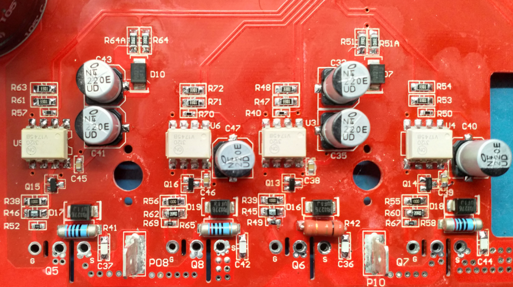
Note: If you look closely, you’ll see all of the 20R0 resistors were replaced with 39R0. There are two 39R0 resistors stacked on top of each other, but you can’t see that in the photo, so they’re actually 19R5 now. I somehow forgot to order the 20R0 resistors but had the 39R0’s in stock. You can also see where I’ve replaced one of the 200R resistors with a leaded type, as I couldn’t source any suitable 200R resistors in that size.
Bench Testing:
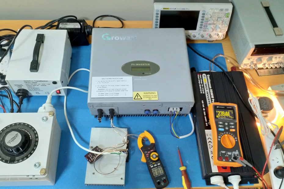
It was time to think about bench-testing the inverter. I wanted all of my testing to be current-limited, in case something went wrong. I didn’t want to connect the inverter to the grid for testing purposes, nor did I want to put ~330V DC across the PV input terminals and hope that didn’t end badly. I also don’t have solar power here, so the smart meter detecting anything that resembles feed-in had to be avoided, so that rules out connecting it to the grid via a ballast of some sort. I’m not sure how I’d explain a feed-in event to the power company.
The bench test setup was using the isolation transformer in the schematic below to do the current limiting. It’s a 5A isolation transformer with a suitable fuse installed. In future I’ll be using a 100W electromagnetic ballast to limit the current, so it’s included in the schematic, but wasn’t actually there when this inverter was tested:

The variac was used to slowly ramp up the voltage and to cut off the PV feed-in to the inverter when the output current of the PV inverter got too high. Photovoltaic panels are isolated from the mains normally, so an isolation transformer was also used.
The next thing to do was emulate the grid to trick the inverter into thinking it was grid connected. I gave this a bit of thought and decided to risk killing a pure sine wave inverter by back feeding it a little. I had a Mishto 2500W/5000W inverter that I never use sitting in it’s box, so used that. There were some scary moments, but nothing went bang (kind of surprising since back feeding such an inverter is asking for trouble).
My understanding of how grid-tie PV inverters work is that they raise the output voltage slightly above the incoming grid voltage, and by doing so are able to feed into the grid. This meant that the PV inverter was going to try to take over powering the test load if it could, and would probably be quite happy to back-feed the Mishto inverter and destroy it.
Using the variac, I was able to regulate how much current the PV inverter could put out, and thus keep the test load partially powered by both inverters. It was a balancing act, and it got scary at times. This is why I’d use a 100W ballast in future, combined with a test load over 100W, so that the PV inverter could never take over powering the test load completely.
Below is a diagram of the emulated “grid” side of the test bench setup:
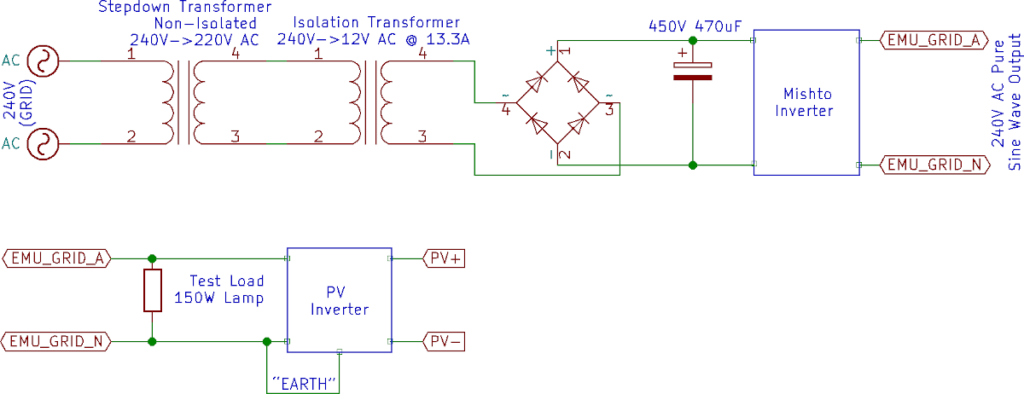
The step-down transformer was used mostly to reduce the output voltage from the large 13.3A transformer feeding the low voltage side of the Mishto inverter. Once rectified and when under no load, the voltage was too high and the Mishto inverter would indicate a fault.
Connecting the PV Inverter earth to the 240V neutral was done as the PV Inverter initially came up with a “PV Isolation Low” message. This I feel is rather dangerous, since the metal chassis of both inverters is now tied to the 240V “neutral”, which may not be safe to come in contact with. Something I considered was instead connecting a 1uF X2 capacitor between the earth and neutral of the PV inverter, to again limit any current flow should something go wrong. I never did it, so don’t know if it would have worked to suppress the PV isolation fault message from the PV inverter (it won’t start up with a PV isolation fault condition).
Test Bench Setup:
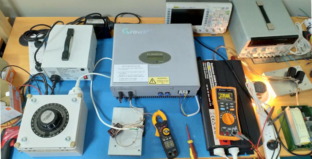
I’d like to find a way to protect the Mishto inverter from being back-fed, but haven’t been able to think up a solution to that so far. If you think you know of one, feel free to clue me in.
Component Values:
Here comes the useful information if you’ve got the skills to do this level of component repair. Since there isn’t a schematic diagram available at this time of writing, I’ve made a list of every component in the H-bridge circuitry, which I expect would be the most likely part of the inverter to fail.
I replaced some additional components out of an abundance of caution, since I didn’t want to do this repair twice. Not when it’s costing $120 each time and risking damage to the main logic board, which could write-off the whole thing. Until a schematic becomes available, I’d suggest you consider going the extra mile if attempting a similar repair.
Logic Board:
U2: ULN2003A (SOIC-8)
Power Board:
C43, C41, C47, C33, C35, C40: 220uF 25V LOW ESR (eg. UUD1E221MNL1GS)
C45, C46, C38, C39: 100nF 50V (0603)
D7, D10: UF1J (DO-41)
R64A, R64, R51, R51A: 20R0 (1206)
R61, R63, R71, R72, R47, R48, R53, R54: 3.3K (1206)
R57, R70, R40, R50: 68B (4.99K, 0805)
U5, U6, U3, U4: FOD3120SDV (8SMD)
Q15, Q16, Q13, Q14: MMBT2907A (Original Marking: 2E, PNP, SOT-23)
R38, R56, R39, R55: 100R (1206)
R46, R45: 0.02R (1206) *
R62, R60: 20R0 (1206)
D17, D19, D16, D18: UF1J (DO-41)
R52, R65, R49, R67: 47K (0603)
R41, R65, R42, R58: 200R (1W(?) Metal Film MELF) **
C37, C36: 220pF 100V (1206)
C42, C44: 470pF 100V (1206)
Q5, Q8, Q6, Q7: IXGH48N60C3D1
Other components I replaced as a precaution:
1x IXGH48N60C3D1 + FOD3120SDV
1x SPW47N60C3FKSA1
2x Song Chuan SCL-1-H-DPNO 12VDC Relays (they both had worn contacts).
* These two resistors are probably just zero ohm links, but the originals were unmarked. As the original resistor that survived measured around 0.02R, I replaced them with 0.02R resistors (P/N: PF1206FRF070R02L). I also checked the original component for inductance, but it wasn’t measurable.
** R42 was damaged slightly. I couldn’t find a suitable replacement, so replaced it with a 200R Vishay PR02, and turned it into a surface mount resistor by bending the leads tightly under the resistor and cutting them short.
Update (29/07/2022): The inverter is still working well, no further problems so far.
Update (04/09/2024): Still working 🙂
